AUNV-TEMPORARY-FORUM
[ main ][ links ][ about ][ help ][ discussions ][ projects ]Inside an Image Tube.
Getting a feel for the inside of an image tube can be difficult if you're one of the many who has never taken one apart. This is a quick article on what exists beneath the plastic boot that hides what lies within.
Although we (mostly) all kind of know what's inside of an image tube, have you ever considered what it all means? Having a good image in your mind helps you understand the technology, it's limitations and the scale on which things occur.
So for those interested, here's a brief journey through a modern Gen3 image tube. And for those who like to have a yardstick to measure things by, the average thickness of a human hair is about 100microns, or 100,000nm or 1 million Angstroms.
The Photocathode.
Most Gen3 tubes have this deep blue photocathode below a glass substrate which makes them relatively easy to identify, although late US Gen2 sometimes have similar colors.
The photocathode is a piece of glass around 5mm thick that's clear on one side and on the other they grow a Gallium Arsenide Crystal ( GaAs ) that acts as the photocathode. That is, it converts photons into electrons.
This is straight photoelectric effect. Gallium Arsenide is a semiconductor and you can make electronics out of it. They make very expensive solar panels out of the stuff also. Excellent for satellites and the like where high efficiency solar cells are needed, but the cost of satellites makes using this expensive stuff worth it.
They grow the photocathode right there on the glass faceplate like how mist forms on glass when you blow on it, except it doesn't evaporate. It grows... Just vapor but it builds up over time.
And they build it up like a layer-cake because it's not just a single piece of GaAs.
You might think that in itself is unusual, but there's more to it than that. First of all you know how they coat optics for riflescopes and the likes? Well that glass window is an optic, so they use a coating, approx 1/4 wavelength ( eg, around 200nm ) of Silicon Nitride to act as an antirelfective surface and pass the light on towards the photocathode.
The next layer to go down is an Aluminium Gallium Arsenide layer about 5 microns ( 5000nm ) thick. This acts as a bandpass filter ( above 600nm ).
Next they grow a single crystal of zinc-doped GaAs that's between 1 and 1.8 microns thick. This is the active layer. Then finally they add a monolayer ( think 1 atom thick ) of Cesium and apply oxygen to convert this to Cesium Oxide. It's this change that causes the band-bending of the GaAs and results in the negative electron affinity ( NEA ) that I mentioned in the Gen4 discussion.
That's a simplification of the process, but consider how thick this photocathode is... Then compare it to a Gen2 photocathode that is about 300nm ( 0.3 micron ) thick. Big difference eh?
The MCP.
The Microchannel Plate is the best-known part of Gen2 and Gen3 image intensifiers. These have been around for decades but even now research is going on to improve them.
They take an etchable glass and surround it with a lead-silicate glass, create a boule and draw it through a glass-fiber furnace. They take a bunch of these glass fibers and put them together ( usually into a hexagonal shape ) and draw them once again and once more stack these together and fuse them. Because the fibers get progressively smaller each time they draw them, they end up with a rod made from millions of glass fibers.
They then slice this at an angle - usually about 6 degrees and into slices approximately 0.3 to 0.4mm thick. These are then etched to dissolve the etchable glass and this produces millions of small holes in the plate at the same angle at which the bundle was sliced. These are the microchannels.
They coat the outsides with a conductive layer of nichrome and the MCP is finished, ready to use ( after a little scrubbing, but that's not for this explanation today ).
HOWEVER, the Gen3 MCP also has an ion barrier film. They float laquer on water and create a self-supporting laquer film by lowering the water onto a supporting frame and letting the laquer dry. Then ( in a vacuum ) they place this on the MCP, coat it with Aluminium Oxide to a thickness of about 30 Angstrom ( 3nm or 0.003 microns ) and sinter this by baking to create an aluminium oxide film over the input side of the MCP.
Kind of like wetting pastry, coating with spices and baking away the moisture.
At 30 angstrom the film will stop any electrons that don’t have enough voltage to push their way through. This is known as the dead-voltage and the result is that not all electrons get through the film. The film stops damaging positive ions that are developed in the MCP during operation from reaching the photocathode, but the downside is that some electrons are stopped from getting to the MCP also.
This effectively reduces the sensitivity of the tube by around 50 percent in a standard filmed tube.
The Screen.
There’s a fair bit about screens that aren’t widely known. The technology dates back to vacuum tubes before WW2 and it’s basically the same as the old CRT TV sets that everyone on this forum knows well.
They call them phosphor screens because they convert electrons to light, but that doesn’t mean they use phosphorus.
In fact, they make them underwater. Imagine mixing all the stuff you need and shaking it up, pouring it into a big glass with the screen substrate and allowing it to settle. That’s how they do it. All the phosphor particles settle on the glass or fiber plate that forms the screen.
Add some sodium silicate or potassium silicate as a binder, some barium acetate as an electrolyte and when it’s settled, let it dry in the air. The optimum thickness for a screen using 8 micron particulates is around 8 micron’s thick. This will allow a resolution of over 100 lp/mm - sufficient for the resolution of the MCP.
Then they deposit an aluminium coating over the screen in argon gas to provide suitable conductive medium and to keep the light from getting back to the photocathode for obvious reasons.
There are other ways to do it, but this gives you an example and probably impresses on you that these guys would make good chefs.
There are quite a number of screens that might be used on a gen3 tube. Two common ones are P20 and P43.
Phosphor screens exhibit two forms of function. Fluorescence and Phosphorescence. Fluorescence is when it lights up when struck by electrons. Phosphorescence is how long it remains lit up afterwards.
P20 is a yellow-green phosphor with a peak output at 560nm. It decays to about 10% brightness in 0.2ms.
P43 is also a yellow-green phosphor with a peak output at 544nm and decays to about 10% brightness in 1.2ms.
This is probably why P43 is more popular as a screen. It’s extended phosphorescence allows the image to appear brighter to the user under extremely low light conditions.
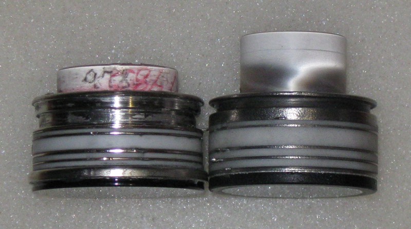
The Fiber Twist.
( as shown above, shorter on the MX10130 that does not have a twist in the screen FO plate. The twist can clearly be seen in the MX10160 on the right. )
Remember the description of how the MCP is made? Well the fiber twist is made the same way, except it isn’t etched.
Fiber Plate is an invention from the 1950’s and it was what made the first starlight scopes possible. It also allowed the glass to be shaped and this reduced the distortion of the tubes as well.
Well, they grab a piece of rod made from the stuff, heat it and twist it 180 degrees. This allows the image to be inverted which simplifies the optics of the scope in which the tube is to be used.
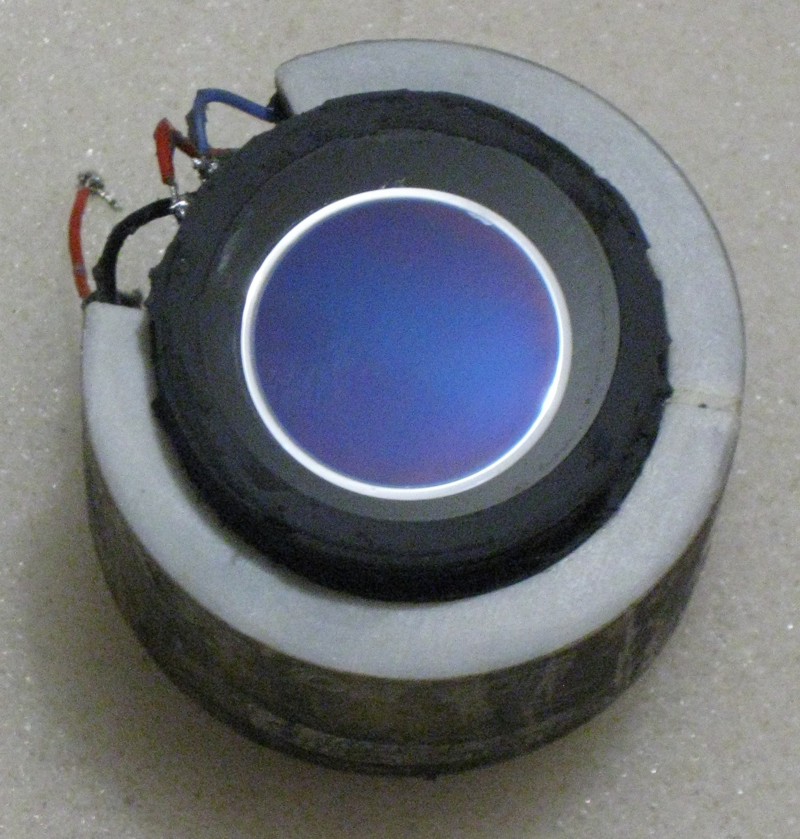
Power Supply.
The power supply is a separate component, but it too fits in the package. It takes 3v and runs this through an oscillator and after building up the voltage to a higher level, it’s put through a cockroft/Walton generator (http://en.wikipedia.org/wiki/Cockcroft%E2%80%93Walton_generator ) to build up the voltages to the required level.
There are three outputs (and one ground) from a power supply.
1. The Screen. This is kept at a potential of around 5000v.
2. The MCP input. This is typically kept at a potential between -200v and -800v.
3. The Photocathode. This is typically kept at a potential around 800v lower than the MCP input - so around -1600v.
The MCP output is kept at ground potential.
In thin-filmed tubes, the photocathode is at about -600v beneath the MCP input and in filmless, it’s approximately -200v below. This voltage variation is most likely necessary to ensure that most electrons make it through the film.
Power consumption of the power supply is around 40ma at 3v. Not much.
The above is an example of a Gen2/3 PSU. The three high voltage lines can all be seen on the left. Yellow is the screen, Red is the MCP and Blue is the Photocathode.
Assembly.
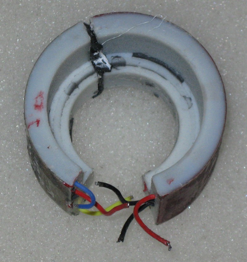
Now you have all the parts, it’s time to put them together. Under a vacuum, they use bellows to hold the pre-assembled parts apart while they activate the GaAs photocathode ( The Cesium oxidising process ) and then they fit the parts, separating the sections with ceramic rings holding apart metal rings that keep everything in place.
Indium ( a soft metal like solder ) seals allow for air-tightness and the process is complete. Small metal tabs stick out through the metal rings and these are soldered to the power supply. The tube is filled with an insulating compound, an elastomer made from silicon. This is also known as the potting.
Then the tube is housed in a suitable form ( eg, Thin Anvis ) for it’s intended purpose.
Inside, the parts are now very close. The photocathode is within a few 10ths of a millimetre of the MCP and the screen is just a few mm away.
This is why the tubes can be damaged by shock. The MCP can flex enough to actually touch the Photocathode. With the voltages involved, this will burn a hole in the photocathode and damage the tube permanently.
Well, I hope this has been interesting. I’ve simplified this process as much as I can. If you have questions, please let me know.
If you would like to get deeply into what makes an image tube tick, I’d recommend a book called “Image Tubes” by Illes P Csorba. It’s not in print anymore but often shows up on Amazon.com as a secondhand book.
David